A PRACTICAL DRIVE CIRCUIT
FOR THE
MT-6010 POWERBLOCK POWER SYSTEM
by
Applications Engineering Staff
POWERTECH, INC.
0-02 Fair Lawn Avenue - Fair Lawn, NJ 07410
ABSTRACT
Featuring Pulse Width Modulation: high efficiency, low cost, single power
supply operation, easily adjustable IB1, and easily adjustable IB2.
Introduction
In all power conversion applications using high-current power transistors,
satisfactory circuit operation depends on good drive circuit design and
implementation. With all switching power supplies, it is important to minimize
power stage switching losses. Good drive circuit design not only reduces
switching losses but improves circuit reliability.
An optimum bipolar drive circuit should provide:
- High di/dt forward base drive (IBl) so as to turn on the power
semiconductor devices quickly.
- Adequate IB1 current to keep the power semiconductor devices in saturation
so as to minimize saturation (VCEsat) losses. This is especially important when
Darlington devices are used because of their saturation voltage.
- Controllable di/dt reverse current drive (IB2) to sweep out stored charge
in the base, thus speeding up device turn-off.
The drive circuit described here provides adjustable forward and reverse
current with a single power supply. It is simple, efficient, and can be
modified to drive a variety of power semiconductors.
Theory Of Operation
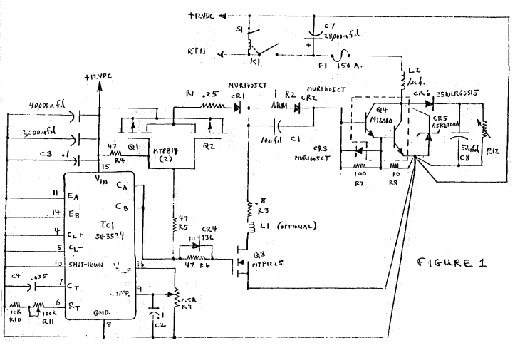
In Figure 1, FET driver transistors Ql and Q2 receive a pulse width
modulated signal from the collectors of the NPN bipolar output transistors in
PWM chip IC1. Transistors Ql and Q2 are operated in parallel. This provides
for greater circuit reliability, lower junction temperature, and lower driver "on"
resistance. With transistors Ql and Q2 "on", forward current Ibl
flows through R2, CR1, Cl, R2, and CR2 before turning on Darlington Q4.
Capacitor Cl serves two purposes. During turn-on, it provides overshoot for IBl
and during turnoff, the energy stored in Cl is used for reverse current (IB2)
for fast turnoff for Darlington Q4.
As the gates of transistors Ql and Q2 go high and they are turning off,
transistor Q3 is turning on. Reverse current IB2 then starts to flow through
R3, Q3, and Darlington Q4. The reverse current IB2, or IB(off), is used to
quickly remove the stored charge carriers from the base regions of Darlington Q4
for fast and reliable turn-off.
Using load-line analysis, forward and reverse drive can be optimized by
adjusting turn-on and turn-off load-locus for minimum switching area.
Integrated circuit IC1, and SG3524, is used as an open loop PWM drive oscillator
in this circuit. Other PWM integrated circuits, as well as a variety of other
circuits, could be used as drive oscillators with this drive circuit.
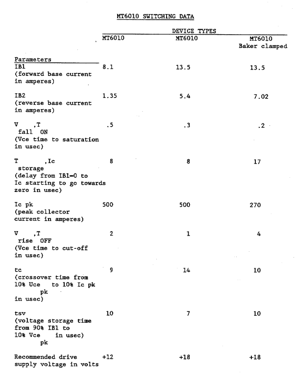
MT-6010 Switching Characteristics
The MT-6010 is susceptible to ISB turn-on second-breakdown, as well as ESB
turn-off second-breakdown. Forced gains above 100 are not recommended. Care
must be taken not to exceed the maximum VBE during device turn-on and VBER
during device turn-off. ISB failure is much more likely to occur when high
di/dt collector current is present during turn-on. Di/dt of equal to, or less
than, 10 amps/usec should necessitate fast IB1 forward current (>8 amps/usec)
and forced gain (hfe) not to exceed 100 at 300 to 500 amperes. Low forced gain
may make Mosfet drive circuitry an absolute necessity depending on the switching
speed that is needed from the MT-6010 for the system requirements.
Notes
1. Base 1 to Base 2 resistance = 100 (R7)
1. 2 Base 2 to emitter resistance = 10 (R8)
Design Hints
- Capacitors used in base drive circuitry should have specified AC ripple
current ratings such as polypropelene, polysulfone, AG oils, and other types.
- Fast recovery diodes (35 - 200 ns.) should be used.
- Non-inductive resistors should be used.
- Forward current IB1 can be adjusted by changing R1 and R2.
- Reverse current IB2 can be adjusted by changing Cl, R3, and L1.
- Changing L1 will vary the di/dt of IB2.
- All FETS may need 15 to 18-volt zeners from gate-to-source to protect
against voltage spikes, depending on the application.
- All FETS may need 35-volt transient suppressors with series diodes from
each Mosfet's drain-to-source, depending on the application.
- Special attention should be paid to short lead lengths in the IB2 (reverse
current) circuit path, so as to maximize IB2 di/dt.
- Some minimum resistance is needed in the turn-off circuit path so as to
keep circuit 'Q' to a low enough value. This keeps reverse VBE and IB2
'ringing' to an acceptable level. Resistance needed with the MT-6010 ranges
from approximately 0.2 ohms to 2 ohms.
Circuit Layout Guidelines
The following checklist should be reviewed. The items that are free of
added cost should be used whenever applicable. The other techniques should be
used if more noise reduction is necessary.
Noise Reduction Checklist
A. Suppressing Noise at Source:
- Enclose noise sources in a shielded enclosure.
- Filter all leads leaving a noisy environment.
- Limit pulse rise times.
- Relay coils should be provided with some form of surge damping. Twist
noisy leads together.*
- Shield and twist noisy leads.
- Ground both ends of shields used to suppress radiated interference (shield
does not need to be insulated).*
B. Eliminating Noise Coupling:
- Twist low-level signal leads.*
- Place low lever leads near chassis (especially if the circuit impedance is
high).
- Twist and shield signal leads (coaxial cable may be used at high
frequencies).
- Shielded cables used to protect low-level signal leads should be grounded
at one end only (coaxial cable may be used at high frequencies with shield
grounded at both ends).*
- Insulate shield in signal-leads.
- When low-level signal leads and noisy leads are in the same connector,
separate them and place the ground leads between them.*
- Carry shield on signal leads through connectors on a separate pin. Avoid
common ground leads between high and low level equipment.*
- Keep hardware grounds separate from circuit grounds.*
- Keep ground leads as short as possible.*
- Use conductive coatings in place of nonconductive coatings for protection
of metallic surfaces.
- Separate noisy and quiet leads.*
- Ground circuits at one point only (except at high frequencies).*
- Avoid questionable or accidental grounds.
- For very sensitive applications, operate source and load balanced to
ground'.
- Place sensitive equipment in shielded enclosures.
- Filter or decouple any leads entering enclosures containing sensitive
equipment.
- Keep the length of sensitive leads as short as possible.*
- Keep the length of leads extending beyond cable shields as short as
possible.*
- Use low-impedance power distribution lines.
- Avoid ground loops.*
Consider using the following devices for breaking ground loops:
- Isolation transformers
- Neutralizing transformers
- Optical couplers
- Differential amplifiers
- Guarded amplifiers
- Balanced circuits
C. Reducing Noise at Receiver:
- Use only necessary bandwidth.
- Use frequency selective filters when applicable.
- Provide proper power supply decoupling.
- Bypass electrolytic capacitors with small high-frequency capacitors.
Separate signal, noisy, and hardware grounds.*
- Use shielded enclosures.
- With tubular capacitors, connect outside foil end to ground.*
*(Essentially free of added cost)
Bibliography
- Blicher, Adolph, Field Effect and Bipolar Power Transistor Physics, New
York, Academic Press, Inc., 1981.
- Ott, Henry W., Noise Reduction Techniques in Electronic Systems, New York,
John Wiley and Sons, 1976.
- Peter, Jean Marie, The Power Transistor in Its Environment, Canoga Park,
California, Thomson - CSF, 1979.
- Pressman, Abraham I., Switching and Linear Power Supply, Power Converter
Design, Rochelle, New Jersey, Hayden Book Company, 1977.
 Back To Products Page